Timing Diagram Basics
Timing diagrams show timing relationships between different signals inside an electronic circuit. They consist of signal waveforms and timing parameters like delays, setups, and holds. The waveforms show how the state of the signal changes with time. Parameters show the cause and effect relationships between signal state changes (signal transitions) and are useful for determining the critical timing paths of a design.
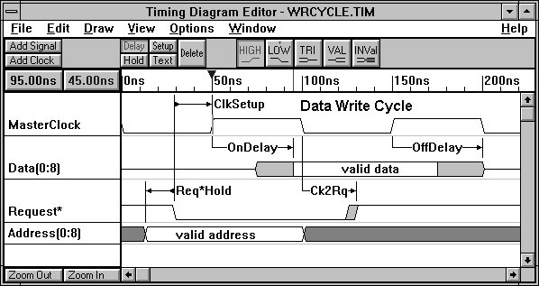
Figure 1 shows a typical timing diagram and an associated timing parameter table. OnDelay, a delay parameter, indicates that when the MasterClock goes high the data on the Data bus will become valid between 25 and 45 ns later. The gray region shows the uncertainty region for when the data may or may not be valid. These uncertainty regions grow in width as a logic value passes through different stages of a circuit. If a logic value pass through two components with a 5 to 10 ns delay, then the resulting uncertainty region is 10 to 20 ns long (5+5, 10+10).
For more information on timing diagrams look at the following pages